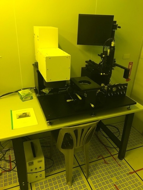
Mask Aligner
Manufacturer: Deya Optronic Co. (德揚光電)
Service:
-
We provide services to transfer a geometric pattern from a photomask to a photoresist on the substrate. The minimum line width can reach 1um.
-
The 5” square photomasks with the period is from 1um to 31um are available in our lab.
Specification:
Contact photolithography exposure tool for 4” wafers. An optimized process can achieve 1 um line/space patterns with a layer-to-layer registration accuracy about 1 um. To operate the lens and the UV lamp, pressure has to set around 5kgf/cm2.
Material Restrictions: Uses 5” square photomasks. Configured for exposure of 4” wafers; smaller chips can be accommodated using a carrier wafer.
Contact:
-
Mr. Alexey Kopeykin
Email: a.kopeykin@gapp.nthu.edu.tw
Phone: +886-3-5162333